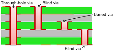
BLIND/BURIED VIA
Vias, that is, copper plated holes, play a key role in the interconnection between layers in a printed circuit board. Generally speaking, vias in PCBs can be classified into the following categories: through-hole via, blind via and buried via. Blind/buried vias are widely applied in SMT (Surface Mount Technology) just to compensate for disadvantages of through-hole vias.

Blind via connects one external layer and one or more inner layers in printed circuit board, responsible for interconnection between top layer and inner layers or bottom layer and inner layers.
Buried vias connect only inner layers inside printed circuit board so that they are invisible just from the outer appearance of a PCB since they are internally “buried”.
Blind/buried vias conform to the density improvement of boards without the need to increase number of layers or board size. Therefore, blind/buried vias are usually applied in HDI PCBs. Put in another way, blind/buried vias can be picked up when you suffer from tight requirement of limited space and through-hole hassles.
Due to our over 20 years’ experience in this industry, Wonderful PCB specializes in manufacturing PCBs with blind/buried vias. Both engineers and manufacturing equipment from Wonderful PCB ensure our full capabilities in meeting the requirements of blind/buried via technology.
Up to now, we’re capable of providing mechanically drilled and laser drilled solutions. When it comes to mechanical drilling, via diameter ranges from 0.2mm to 0.4mm while 0.1mm for laser drilling.
Based on your project’s requirements, you can choose corresponding drill diameters in the items while getting an instant quotation for PCBs. For more information about blind/buried vias, we’re always available at wonderful@wonderfulpcb.com.

