

- Brand Name: Customized
- Min.Order Quantity: No
- Supply Ability: 30~50 thousand ㎡/Month
- Port: Shenzhen
- Service: EMS/OEM/ODM
- Payment Terms: T/T,Paypal,WU etc.
- Layer: 6
- Base Material: FR-4
- Copper Thickness: 1oz
- Board Thickness: 1.6mm
- Solder mask color: Blue(can customized)
- Component labeling color: White(can customized)
- Surface Finishing: ENIG
- Service type: Full assembled services
- Application: Consumer electronics products
- Test: E-test,AOI,X-ray,Function test
- Assembly Tech: DIP and Wave Soldering,SMT and Reflow Soldering
PRODUCT DETAIL
CHINA PCB assembly service SMT PCBA Manufacturer for electric appliance
Advantages
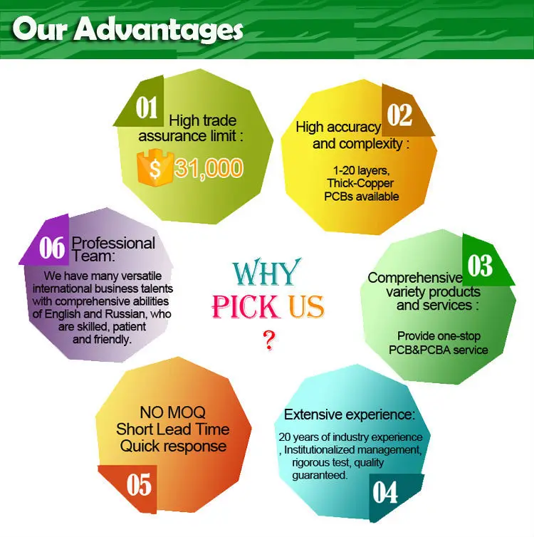
– No MOQ
– OEM services provided
– Heavy copper PCB, Heavy gold PCB, Blind / Buried via PCB, High layer count PCB manufacturable
– Factory direct price
– Replying with price in one working day
– Shipping within 24 hours
– Certificate: ROHS, UL, ISO9001-2000, ISO14001,SGS Lead-Free
Our PCBA Capability
SMT, PTH, mixed technology
SMT: 2,000,000 solder joints per day
DIP: 300,000 joints per day
Ultra fine pitch, QFP, BGA, μBGA, CBGA
Advanced SMT assembly
Automated insertion of PTH (axial, radial, dip)
Cleanable, aqueous and lead-free processing
RF manufacturing expertise
Peripheral process capabilities
Pressfit back planes & mid planes
Device programming
Automated conformal coating
For E-Test
Universal Tester
Flying Probe Open/Short Tester
High power Microscope
Solder ability Testing Kit
Peel Strength tester
High Volt Open & Short tester
Cross Section Molding Kit With Polisher
| If you need PCB assembly service as well, could you give us following information? | |
| 1. | Gerber file of the bare PCB board |
| 2. | BOM(Bill of material) for assembly |
| To short the Lead time, please kindly advise us if there is any acceptable components substitution. | |
| 3. | Testing Guide & Test Fixtures, if necessary |
| 4. | Programming files & Programming tool, is necessary |
| 5. | Schematic, if necessary |
Our Production Capability for PCB
| Number of Layer | 1 – 20 Layer |
| Maximum Processing Area | 680 × 1000MM |
| Min Board Thickness | 2 Layer – 0.3MM ( 12 mil ) |
| 4 Layer – 0.4MM ( 16 mil ) | |
| 6 Layer – 0.8MM ( 32 mil ) | |
| 8 Layer – 1.0MM ( 40 mil) | |
| 10 Layer – 1.1MM ( 44 mil ) | |
| 12 Layer – 1.3MM ( 52 mil ) | |
| 14 Layer – 1.5MM ( 59 mil ) | |
| 16 Layer – 1.6MM ( 63 mil ) | |
| 18 Layer – 1.8MM ( 71 mil ) | |
| Finished Board Thickness Tolerance | Thickness ≤ 1.0MM, Tolerance: ± 0.1MM |
| 1.0MM ≤ Thickness ≤ 6.5MM, Tolerance ± 10% | |
| Twisting and Bending | ≤ 0.75%, Min: 0.5% |
| Range of TG | 130 – 215 ℃ |
| Impedance Tolerance | ± 10%, Min: ± 5% |
| Hi-Pot Test | Max: 4000V/10MA/60S |
| Surface Treatment | HASL, With Lead, HASL Free Lead |
| Flash Gold, Immersion Gold | |
| Immersion Silver, Immersion Tin | |
| Gold Finger, OSP |
We provide OEM services to all sorts of printed circuit board assembly as well as electronic encased products.
Contact us to check out full details, we will reply to you with prices in one working day!
Contact us to check out full details, we will reply to you with prices in one working day!

1.Which type of PCBs do you expert in?
We are specialized in producing HDI multilayer blind, BGA, impedance, half-hole, double-sided, single-sided, etc.
2.Experience?
We are OEM on PCB boards with experience over 15 years.
3.What is your Lead time?
Lead time is usually punctual here, for some special situation, we can also advise customer in advance to avoid any inexpectation or loss at customer side.
4.What is your testing policy and how you controle the quality?
For sample, usually tested by flying probe; for PCB Volume over 3 square meters, usually tested by fixture, this will be more faster. Due to there’s many steps to PCB production, we usually do inspection after every step.
5.What is your certificate?
ISO9001, ISO14001, UL, RoHS report. We can provide the report of raw material based on customer’s requirement.
6.What is your package?
With Inner vacuum package and out carton.
7.PCB shipment?
This is depend on customer, sometimes we ship through our forwarder, who is also the agency of DHL, TNT, UPS, Fedex, and so on. Our forwarder can provide too much better freight cost than we get directly from those express enterprise.
8.What is your produce ability?
Our ability is average 40,000 square meters per month.
9.I only have the pcb sample, not pcb file, can you produce it for me?
Yes, we can copy file based on your sample, this file names gerber, and production then is accorded to gerber file.
10.Can you design gerber file?
We can design gerber file if customer can provide us schematic, schematic sample can also be provided if customer want.
11.What kind of PCB file format can you accept for production? What CAM software do you use?
We accept Gerber file for production. CAM350, GENESIS, UCAM, GC-CAM, V-2000.
12.Will you allow me to put several part number together into one panel?
Yes, this is usually happen in we factory, this way can help customers reduce some cost and to a certain degree, it can help reduce some assembly cost.
13.What material brand you use for your PCB?
KB, SL, NANYA, TACONIC, ROGERS and so on.
14.What is your minimum order quantity?
We have no limitation on MOQ, prototype, medium volume and large volume are all acceptable.
15.Will RoHS Lead-Free Custom Spec. Boards be marked with lead-free symbol?
Yes, can, but need customer to specify this requirement in file.
16.Are my design files safe when I submit them to you for manufacturing?
Any customer’s file will be protected very well here in our factory and we will not let any third party know. We can sign NDA with you.
17.What is the largest PCB size you can fabricate?